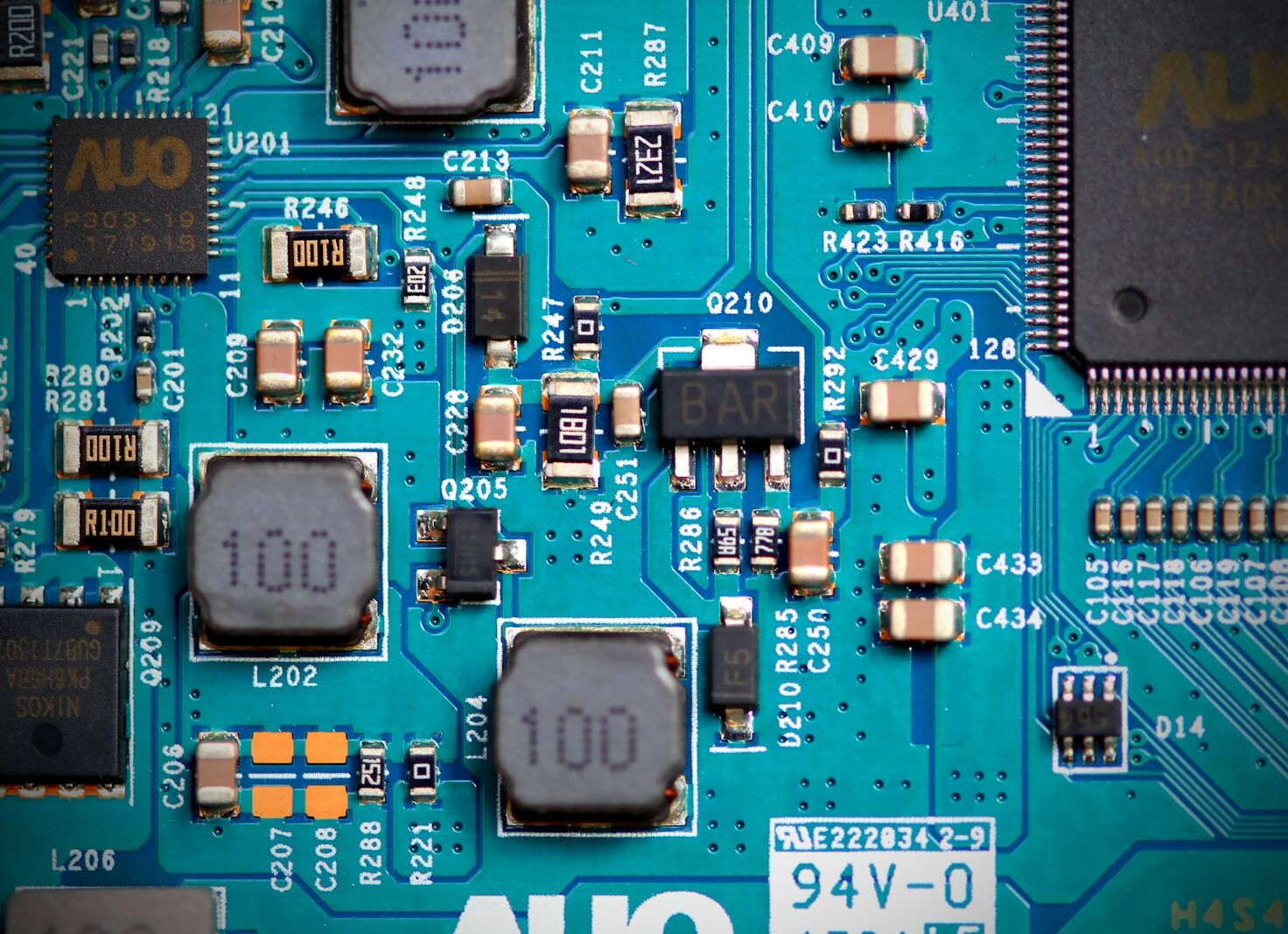
R&D Roadmap

EPSOL is building a systematic R&D roadmap based on the market size  and the recent technological development trend. From the field you are currently focusing on to the next generation of technologies that will lead the future market, you can see EPSOL’s innovative

R&D Roadmap for Semiconductor Materials

Technology Roadmap for Ultra High Performance Semiconductor Packaging

EPSOL is leading the market by providing optimal solutions in line with the trend of high density, high integration, and miniaturization of semiconductor PKG.

a close-up of a circuit board

Recent Development Trend

  • High density / High integration

    Technology that enables high-density packaging by stacking multiple chips.

  • Smaller / thinning

    Ttechnology to minimize the size and thickness of electronic devices.

  • Low loss power

    Material technology that increases power efficiency

  • High-speed transmission

    Technology that improves data transmission speed by minimizing signal loss.

  • Wide I/O

    TSV technology enables wider bandwidth data transmission

2014 ~ 2017

Since 2014, we have been developing 2D PKG materials such as Lead On Chip / Lead Locking tape and Dicing Film.

  • LOC / LLT

    Adhesive material used to attach semiconductor chips to substrates.

  • Dicing Film

    Adhesive film used to cut semiconductor wafers precisely.

  • QFN Tape

    Adhesive tape used to prevent mold leakage in the QFN type packaging process.

  • DAF(Die Attach Film)

    Adhesive film used to attach semiconductor chips directly to a substrate or to stack chips.

2020 ~

We have developed materials used in TSV  technology for high density, high integration. We have gone beyond conventional technology and aimed to develop materials for high performance.

  • TSV Temporary Bonding Materials

    Adhesive material for temporarily bonding and debonding the device wafer in the TSV process.

  • Non Conductive Film

    Nonconductive adhesive film that fills the space between stacked chips in the TSV process.

  • Backgrinding Film

    Adhesive film applied in the grinding process to thin the thickness of semiconductor wafers.

  • Spacer Film

    Adhesive film to secure space between stacked chips in a stacked package

  • Molding Film

    Adhesive material used for final package molding in the FO-WLP packaging process.